Portfolio/Johns Hopkins University

Engineering Portfolio

Selected projects in RF, analog, and mixed-signal design completed at Johns Hopkins University and Texas Tech University.

Two-Stage X-Band GaAs FET MMIC Power Amplifier chip layout

10 GHz WIN GaAs FET MMIC Power Amplifier Design & EM-Verified Layout

EN.525.803 — Special Project: Electrical and Computer Engineering Thesis
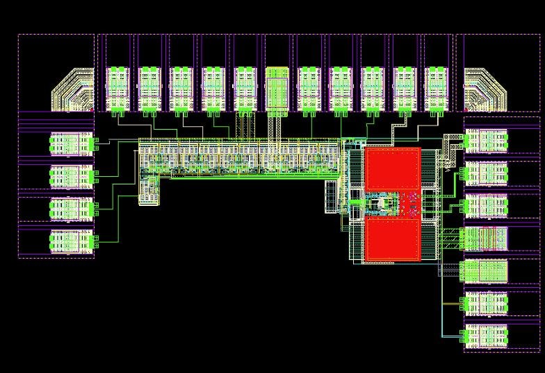
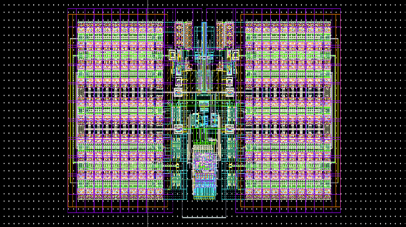
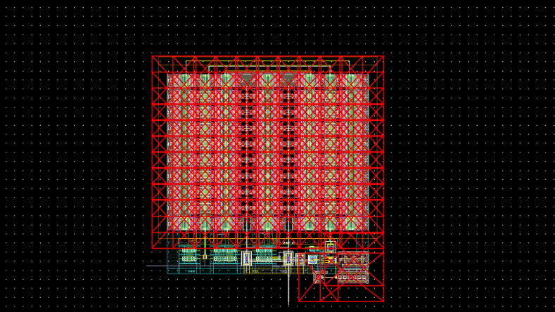
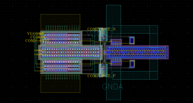
01

A thesis-level design study investigating whether a 10 GHz X-band two-stage GaAs FET MMIC power amplifier can be effectively realized in a process optimized for higher-frequency operation. Developed in Keysight ADS using the WIN MMIC process library, the project covers device screening, bias network synthesis, driver/output-stage sizing, input/interstage/output matching, harmonic-balance power optimization, wideband stability verification, and ADS Momentum EM co-simulation of layout-sensitive structures. The design targets 18.6 dB small-signal gain, 28.2 dBm P1dB, 29.4 dBm Psat, and 31.5% PAE across a 9.5–10.5 GHz X-band passband, with layout planning and DRC review for a compact industry-style MMIC die implementation.

View DOEThesis Report: Pending
SAR ADC full layout — TSMC 65 nm CMOS
SAR ADC top-level layout view
Capacitor DAC array layout
Dynamic comparator layout

100 MS/s SAR ADC Design in 65 nm CMOS

EN.525.732 — Advanced Analog Electronic Circuit Design

02

Designed and evaluated a 100 MS/s Successive Approximation Register ADC in a TSMC 65 nm GP CMOS process. The project implemented a monotonic switching architecture, capacitor DAC, bootstrapped sampling switch, dynamic comparator, asynchronous SAR control logic, layout integration, and post-layout simulation. At a 1.2 V supply, the ADC achieved 59.0 dB SNDR, consumed 0.685 mW, and produced an 11.72 fJ/conversion-step figure of merit, demonstrating an efficient high-speed, low-power mixed-signal converter design.

Power Amplifier Experimental Layout schematic

MACOM GaN HEMT RF Power Amplifier Design & PCB Fabrication Implementation

EN.525.775 — RF & Microwave Circuits II

03

Designed and implemented a 3 GHz RF power amplifier using a MACOM CGHV1J006D GaN HEMT on Rogers 4350B. The project covered the full RF power amplifier design flow, including DC FET characterization, class-AB bias selection, stability analysis, load-pull optimization, input/output matching, harmonic-balance simulation, microstrip PCB layout, and large-signal performance validation. The final design achieved approximately 16.5 dB small-signal gain, 30.5 dBm output power at 3 dB compression, and about 22% PAE at 3 GHz while fitting within a 4 in × 4 in board constraint.

Coupled band-pass filter microstrip layout on RO4350B

5.8 GHz Rogers RO4350B Microstrip Filter Design & PCB Fabrication Implementation

EN.525.774 — RF & Microwave Circuits I

04

Designed and implemented 5.8 GHz microstrip RF filters on Rogers RO4350B using Chebyshev filter synthesis, Richards' transformation, Kuroda identities, and ADS microstrip modeling. The project included both a coupled-line bandpass filter and a five-stub low-pass filter, covering ideal lumped prototypes, distributed microstrip conversion, PCB layout, fabrication, and measured S-parameter validation. Post-fabrication analysis identified layout and DFM issues such as spacing tolerances, milling effects, and unintended trace discontinuities, providing practical insight into RF filter realization beyond ideal simulation.

Low Noise Amplifier 3GHz PCB layout — Khalil Blaine

RF Low-Noise Amplifier Design & PCB Fabrication Implementation

EN.525.775 — RF & Microwave Circuits II

05

Designed and implemented a 3 GHz RF low-noise amplifier using an Infineon BFP420 SiGe RF transistor on Rogers RO4350B. The project covered the full RF design flow, including DC biasing, noise optimization, input/output impedance matching, broadband stability verification, microstrip PCB layout, fabrication, and post-fabrication RF testing. Performance was validated through measured S-parameters and noise figure analysis, with simulation-to-measurement comparison used to identify layout parasitics and guide redesign improvements.

Sequential Logic, Finite State Machines & VLSI Complexity

Texas Tech University — Master of Engineering Thesis

06

Modern communication devices, aircraft systems, power grids, supply chains, and computing platforms are all products of complex engineering systems. Although this complexity is often invisible in daily life, it is enabled by the interaction of multiple engineering disciplines and technologies, extending down to the smallest architectural elements of modern computers. In VLSI design, this complexity is especially evident in the large number of possible combinations among individual chip components. This report defines sequential logic, examines its role within complex engineered systems, reviews selected industry challenges associated with the slowing of Moore's Law, and presents a real-world application problem using finite state machines, sequential logic, and algorithms.

Gate-level VLSI schematic for CNN accelerator — XOR, NAND, half-adder, and multiplier datapath

Digital CNN Accelerator Architecture for VLSI Hardware

Texas Tech University — Master of Engineering (ECE 5310)

07

Developed a gate-level VLSI architecture for a convolutional neural network compute path, implementing the core multiply–accumulate operation used in AI/ML inference hardware. The design decomposed convolution into reusable digital building blocks — XOR and NAND logic, half-adder structures, flip-flops, an 8-bit multiplier, a 32-bit adder, and a register-based running-sum datapath. The final system demonstrated a working simulated CNN computation flow, with measured block-level timing including a 0.7 ns XOR delay, 1.5 ns adder delay, 11 ns multiplier delay, and 33 ns 32-bit adder delay. The project connects VLSI fundamentals to accelerator architecture, AI inference datapaths, MAC-unit design, timing analysis, register-based accumulation, and optimization tradeoffs for high-throughput digital compute systems.